Life with a 51 year old CDC 6500

The CDC 6500 has led a rough life over the last 6 months or so: way back on the afternoon of July 2, 2018, I got an email from the CDC’s Power Control PLC telling me that it had to turn off the computer because the cooling water was too hot! A technician came out and found that the chiller was low on refrigerant. He brought it back up to the proper level, and went away. Next morning it was down again.

After much gnashing of teeth and tearing of hair, it was determined that the compressor was bad in the chiller. “We’ll have a new one in 5 weeks!” The new one turned out to be bad too, and so another was ordered, that was easier to get. Only about 3 weeks, instead of the 8 that the official one took. That worked for a few weeks, and the CDC went down again because the water was too hot.

This time it was very puzzling because as long as the technician was here, it worked fine. He spent most of a morning watching it, decided it was OK, and left, but he didn’t make it to the freeway before it went down again. He came back, and watched for the rest of the afternoon, and found that the main condenser fan would overheat, and shut down, causing the backup fan to come on. The load wasn’t very high, so the backup fan had to cycle on and off, while the main fan motor cooled off. This would go on for a while, till both motors were off at the same time, and then the compressor would go over pressure because the condenser fans were off, and the chiller would stop cooling, resulting in the “Water too HOT” computer shutdown.

Another week went by waiting for replacement fan motors from the chiller manufacturer, with no luck. Eventually we gave up and got new fan motors locally, installed them and the chiller has been working since. While the CDC didn’t seem to mind being off for 102 days for the compressor problem, it didn’t like being off for 3 weeks while we fiddled with the fans.

Both when it was off for 102 days, and this time, we found that Bay 1 was low on refrigerant. The first time we just filled it up, but the second time we looked closer, and found that there is a small leak where the power wires go into the Bay 1 compressor. The compressor manufacturer, the same guys that made the chillers compressor, will gladly sell us a new compressor, but the parts for the 50 year old, R12 compressor, are no longer available. We are working on that, but I haven’t heard that we found the parts yet.

Back to more recent times: now that the chiller is chillin’, and the CDC’s cooling system is coolin’, why isn’t the computer computing?

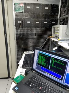
Let’s run some diagnostics and see what happens: I try to run my CDC diagnostic tape, but the machine complains that Central Memory doesn’t seem to be available. No, I didn’t run the real tape drives, I ran the imaginary one that uses a disk file on a PC to pretend to be  a tape drive. Anyway, that didn’t work, so I flip the zillion or so Dead Start switches in my emulated Dead Start panel, to fire up my Central processor based memory test, and get no display at all! This is distinctly unusual. Let’s try my PP based Central Memory test: That seems to work till it finishes writing all of memory, then the display goes blank. Is there a pattern here?

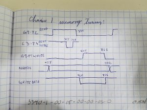
I put a scope probe on the memory request line inside the memory controller in Chassis 3, and find that someone is requesting memory every possible cycle. There are four possible requests: the Peripheral Processors as a group get a request line, each Central Processor gets a request line, and the missing Extended Core Memory gets a request. Let’s find out who it is: the PP’s aren’t doing it, neither of the CP’s are doing it, and the non-existent ECM isn’t doing it. Huh? Nobody is wants it, but ALL of it is getting requested!

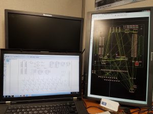
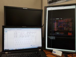
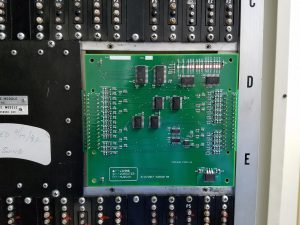
I am going to step back a little bit, and try to explain why it sometimes takes me a while to fix this beast. This machine was designed before there were any standards about logic diagrams. Every manufacturer had to come up with their own scheme for schematics. Here is one where I found a problem, but we will get to that in a bit.

Now when there are two squares with one above the other, and arrows from each going to the other, those are flip-flops. When you have a square, or a circle with multiple arrows going into it, that is a gate. Which one is an “or” gate, and which one is an “and” gate? Sorry, you have to figure out that for your self, because the CDC documentation says either one can be either one. The triangle with a number in it would be a test point on the edge of the module. The two overlapping circles, kind of like an elipsis, indicate that is a coax cable receiver, as opposed to a regular twisted pair signal. A “P” followed by a number indicates a pin of the module.

This module receives the PP read and write signals from the PP’s in chassis 1, on pins P19 and P24. On the right side of the diagram, you can see where all the pins connect. If we look at pin 24, we can see it connects to W07 wire 904, and pin 19 is connected to W07-903. The W “Jack”s are coax cables, the other letter signals go somewhere inside this chassis.

Really, what we are looking at here, is that a circle, or a square is the collector pull-up resistor of one or more silicon NPN transistors. the arrow heads are the base of the transistors, and the line coming into the head has a base resistor in it. If there are three arrows coming into a square, like at the bottom, those three 2n2369 transistors all have their collectors tied together, with one pull-up resistor. I could be slow, because it took about 6 months before I felt I was at all fluent in reading these logic diagrams.

Now we have to talk about the Central Memory Architecture a bit. The CDC has 32 banks of 16K words of memory. Each of these banks is separate, and they can be interleaved any way the 4 requestors ask for them. At the moment, I am only running half of them, because there is something wrong with the other half. Each of these banks does a complete cycle in 1uS. The memory controller in chassis 3 can put out an address every 100nS, along with whether it is for a read or a write. This request goes to all banks in parallel. If the bank that it points to is available, he will send back an “accept” pulse, and that requestor is free to ask for something else. If the controller doesn’t get an “accept” he will ask again in about 400nS. There is a bunch of modules involved in this dance, and it is a big circle.

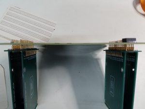
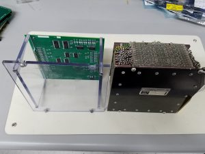
A little more background: This machine was designed before there was such a thing as plated through holes on printed circuit boards. The two boards in each module were double sided. What they did when they needed to get to the other side of a PCB, was they would put a tiny brass rivet in the via hole, and solder both sides.

What I eventually found was that the signal from P23 of the module in 3L34, wasn’t making it to pin 15! There was a via rivet that wasn’t making its connection to the other side of the board. I re-soldered all the vias on that module, and now we were only requesting memory when someone wanted it!

Now that we can request memory and have a reasonable chance of it responding correctly, it is on to testing memory. I loaded up my CP based test, and it ran… for a while. Then it quit, with  a very strange error. The test uses a single bit, and its complement to check the existence of every location of memory. It will read a location, and compare it with what should be there, and put the difference in a second register. Normally I would expect a single bit error, or maybe 12 bits if a module failed that way. The result looked like 59 bad bits, or the error being exactly the same as what it read. Usually this is because the CPU that is running the test is miss-executing the compare instruction.

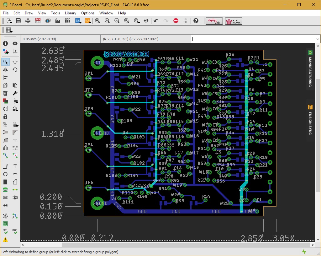
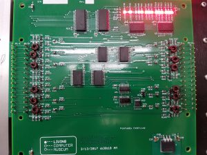
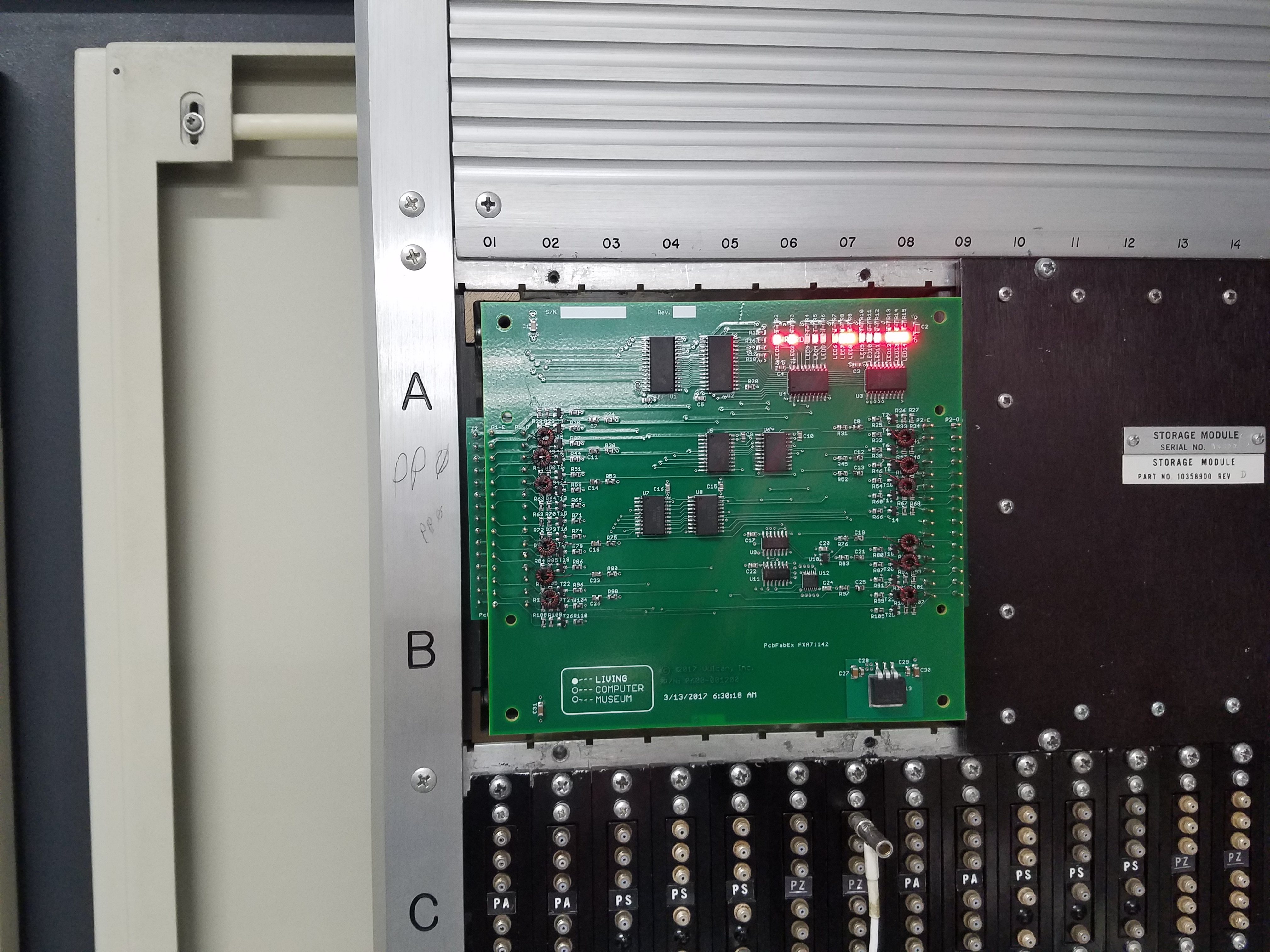
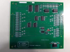
While I was thinking about that, I ran Exchange Jump Test to see what that said. A PP can cause a CP to swap all its registers, including the Program Counter with the contents of some memory that the PP points to. This is called an Exchange Jump. The whole process happens in about 2.6uS as it requests 16 banks of memory in a sequence. This works the memory pretty hard. Exchange Jump Test (EJT) would fail after a while, and as I looked at the results, I noticed that it was usually failing a certain bit in bank 7. I checked, and noticed it was an original memory module, so I looked at my bench and found I didn’t have any new ones assembled, so I had to put the sides on a couple of finished PCB assemblies, and test them. I then swapped out the old memory in bank 7 with a new semiconductor memory, and EJT passed!

I then checked to see if my CP based memory test worked, and it did too. We are back in Business after over 5 months. I am keeping my fingers crossed in the hope that the chiller stays alive for a while.

Bruce Sherry

New peripherals for old Computers

Five years ago, when we were getting done with restoring our PDP10-KI, we were running out of working disk drives to run it from. We were down to one set of replacement heads, two working drives, and we didn’t have a source for new ones. We found some folks that said they could rebuild the packs, but it turned out that they couldn’t re-write the servo surface, so if we lost that we were in trouble.

Alright, what else can be done? The Digital RP06, the drive of choice for the KI, has lots of registers available from the MASBUS. The MASBUS is kind of a UNIBUS, with a synchronous data channel for moving the actual data. We had been having difficulty keeping track of everything on an existing project, so I looked into doing things a different way.

My idea was to use an FPGA, (Field Programmable Gate Array) to emulate the behavior of the control unit inside the RP06. This is like the ease of writing software, but for hardware. No wires to change, no cuts, when I mess up the logic. The PC would be responsible for handling the actual data for the disk, or possibly tape.

I spent a while poking around the Internet looking for an FPGA card that would plug into a PC. There were a lot of expensive, and some less expensive evaluation boards out there. I eventually happened across http://mesanet.com/. I had heard of these folks before from my experiences with LinuxCNC, which runs my milling machine at home. These folks have been doing this for a long time, and since they have to deal with industrial environments and big motors, their products are very robust.

For the MASBUS Disk Emulator, (MDE), I chose the Mesa 5i22 card, which has 96 I/O’s I can play with, and a Spartan3 Xilinx FPGA. The 5i22 doesn’t remember what the Xilinx configuration is, so the PC pours in the correct bits each time.

Bob Armstrong, down in the Silicon Valley, wrote all the software for the PC, and we eventually emulated RP06’s, RP07’s which hold twice the data, and TU77 tape drives. Here is a picture of our main collection of MDE’s.

There are 3 Industrial PCs, and 8 MASBUS Cable Driver/Receiver boxes. These are running both PDP10-KL’s, and the PDP10-KS’s. There is a real TU78 tape drive, to the left of the MDE rack. The PDP10-KI, and the PDP11/70 each have their own located elsewhere in the museum.

I also used the 5i22 for all of the emulations that we needed for the CDC6500:


Here we have one Industrial PC, and 6 6000 series channel attach Driver/Receivers, along with one 3000 series channel Driver/Receiver. We emulate the dead start panel, the DD60 Display, Tape drives, disk drives, printers, card readers, card punches, the serial terminal interface and the 6681 channel converter so we could talk to the real 405 card reader. Bob Armstrong also wrote the PC code for all these emulations.

Jeff Kaylin has also used 5i22 cards on the Sigma 9, with Bob doing the software, and Craig Arno and Glen Hermannsfeldt used one to emulate the card reader and punch on the IBM 360/20.

All is not sweetness and light however, after making the 5i22 for over 10 years, the parts are getting hard to obtain, so Mesa Electronics has stopped production of that board. We ordered all their remaining stock of the 5i22s. They no longer make the 5i22, but they make lots of other similar boards, so we ordered some 7i61’s and 7i80’s to play with.

The 7i61 uses USB to talk to a PC, and has 96 I/O’s to play with. The 7i80 uses Ethernet to talk to the PC, but only has 72 I/O’s. To conserve 5i22’s, I converted my CDC 6681 6000 to 3000 channel converter to the 7i61 because it needs all 4 cables for 96 I/Os. I used my code, along with open source code from Peter Wallace, of Mesa Electronics, to load my code into the serial flash chip on the 7i61, so the PC is no longer involved in the 6681 emulation. After turning on the power to the Mesa card, it knows how to be a 6681 automagicly! I no longer have to remember to type the proper incantation into the PC to get it loaded up, this is a GOOD thing!

After getting the CDC 6500 working, I had several broken modules that I wanted to fix, so I built a Module tester, using the 7i80 card:

You can see the 7i80-HD card under the cables down from the test card.

It took me a while to collect the appropriate bits of Peter Wallace’s code, so that I could have the Ethernet interface live in with my test code, all at the same time, but perseverance pays off, and it all works now. I have fixed 4 out of 5 broken UA modules, and I know why I am not going to fix the other UA, and the ED module that I replaced in CP1.

I have to confess: the module plugged into the tester, is not really from the 6500, but it is the same form factor, and technology.

I love these Mesa Electronics “Anything I/O” cards! As their name says, I can teach them to be most Anything!

Bruce Sherry 20180418.

That Pesky PS Module!

When we last left our hero, he had re-soldered all the Via rivets on one of the 510 “PS”, core memory sense amplifier modules in the CDC6500, and the machine was working.

That lasted about a day, and the memory went away again. What was wrong this time? You guessed it, bit 56 in bank 36 was bad again. Third time is the charm: I am going to replace this module! I head off looking for a spare PS module. Where did we put all those spare parts we got with the machine? Oh wait, we didn’t get any spares with the machine. Bummer!

This is where I get to practice my “MAD Skillz”, and make some spare PS modules. What does a PS module look like? What does CDC give me?

On the left side we have an actual schematic of one of the 4 amplifiers on the module, YAY! Having been around this block before, I take apart the offending module and check to see if it matches. Wiring wise, yes it matches, but the values have been changed to protect the innocent.

After a while playing with the newest version of Eagle, I ended up with this:

The easy part is done, now the fun starts! The circuitry for the module is split between two printed circuit boards, one that connects to the odd pins on the connector, and has odd numbered transistors, and one for the even bits. Eagle really doesn’t understand this, so I have to fool it. First I put test points on each side of all components that go between the boards. I have to then add in the wire jumpers that also go between the boards, and I end up with another schematic:

I take this schematic and duplicate it into odd and even sides, then I write an Eagle script to delete all the between boards components, and all the test points that belong on the other board. Here is what the schematic for the odd board looks like, pretty terrible:

Now I have two schematics: PS_O and PS_E, and I do the PC layout thing. I have the original boards to use as an example, which I follow very closely so that timing and signal integrity will be as close as I can to the original module. Here are pictures of the odd and even layouts:

But wait, I’m not done yet! Remember Eagle doesn’t understand the whole module. I now have to verify that the two boards, together with all the components that go between, match that original schematic I started with.

I go over every line on the board pairs, and the schematic highlighting them as I go, until EVERYTHING is highlighted.

Done yet? Grumble, grumble: No! I have forgotten to identify which end of the diodes and polarized capacitors have the band on them! If I want them assembled properly, I guess I should do that before they go out to FAB!

Back to the PC mines…

Bruce Sherry 20180201 10:57AM

Chasing the Pesky Ratio!

It seems like I did something really silly! I had to come up with some goals for 2018. I hate this time of year, I think everybody does. OK, what can I put down that is measurable and achievable? How about keeping the CDC6500 running more than 50% of the time? That might work. Oops, did I hit the send button?

“Hey, Daiyu: How do I tell what users have been on the machine?” Daiyu Hurst is my systems programmer, who lives Back East somewhere. If it is on the other side of Montana from Seattle, it is just “Back East” to me. She lives in one of those “I” states, Indiana, or Illinois, not Idaho, I know where that is. After a short pause, she found the appropriate incantations for me to utter, and we have a list of who was on the machine, and when they logged in. I had to use Perl to filter out those lines, but that was pretty easy.

What is all this other gobble-de-gook in this file:

 03.14.06.AAAI005T. UCCO, 4.096KCHS. 
 03.16.09.AAAI005T. UCCO, 4.096KCHS. 
 03.18.11.AAAI005T. UCCO, 4.096KCHS. 
 03.20.12.AAAI005T. UCCO, 4.096KCHSUCCO, 4.096KCHS. 
 05.00.30.SYSTEM S. ARSY, 1, 98/01/24.
 05.00.30.SYSTEM S. ADPM, 11, NSD.
 05.00.30.SYSTEM S. ADDR, 01, LCM, 40.
 05.00.44.SYSTEM S. SDCI, 46.603SECS.:
 05.00.44.SYSTEM S. SDCA, 0.032SECS.:
 07.32.30.SYSTEM S. ARSY, 1, 98/01/24.
 07.32.30.SYSTEM S. ADPM, 11, NSD.
 07.32.30.SYSTEM S. ADDR, 01, LCM, 40.
 07.33.07.AAAI005T. ABUN, BRUCE, LCM.:
 07.33.37.SYSTEM S. SDCI, 116.108SECS.:
 07.33.37.SYSTEM S. SDCA, 0.078SECS.:
 07.33.37.SYSTEM S. SDCM, 0.005KUNS.:
 07.33.37.SYSTEM S. SDMR, 0.004KUNS.:

The line with “ARSY” in it is when I booted the machine, at 5:00 this morning, from home. It crashed before I got in, and I booted it again at 7:32. Then we get to 7:33:07, and the “ABUN” line, where I login from telnet.

From the first few lines we can see that the machine appeared to still be running and putting things in its accounting log at 3:20, but it crashed before it could print a message about 3:22.

OK from this, I can mutter a few incantations at PERL, and come up with something like:

1054 Booted on 98/01/23 @ 07.39.30
 Previous uptime: 0 days 5 hours 59 minutes
 Down time: 0 days 17 hours 28 minutes
 1065 Booted on 98/01/23 @ 13.38.30
 Previous uptime: 0 days 1 hours 23 minutes
 Down time: 0 days 4 hours 35 minutes
 1068 Booted on 98/01/23 @ 14.12.30
 Previous uptime: 0 days 0 hours 0 minutes
 Down time: 0 days 0 hours 33 minutes
 1392 New Date:98/01/24
 1498 Booted on 98/01/24 @ 05.00.30
 Previous uptime: 0 days 13 hours 7 minutes
 Down time: 0 days 1 hours 40 minutes
 1503 Booted on 98/01/24 @ 07.32.30
 Previous uptime: 0 days 0 hours 0 minutes
 Down time: 0 days 2 hours 31 minutes

Last uptime: 0 days 0 hours 1 minutes

Total uptime: 2 days, 1 hours 37 minutes in: 0 months 7 days 0 hours 14 minutes
Booted 15 times, upratio = 0.29

Here is where the hunt for the Pesky Ratio comes in: See that last line? In the last week, the CDC has been running 29% of the time. That isn’t even close to 50%. I KNOW the 6000 series were not the most reliable machines of their time, but really: 29%?

What has been going on? A week ago, I was having trouble keeping the machine going for more than a couple of minutes. Finally, it occurred to me I might see how the memory was doing, and it wasn’t doing well. It took me a while to find why bit 56 in bank 36 was bad. I had to explore the complete wrong end of the word for a while, before I realized that end worked, and I should have been looking at the other end. I chased it down to Sense Amplifier (PS) module 12M40. When I put it on the extender, the signal would come and go, as I probed different places. I noticed that I had re-soldered a couple of via rivets before, so I re-soldered ALL the via rivets on the module.

What do I mean “via rivets”? In those days, either one of two things were true: either they didn’t have plated through holes in printed circuit boards, or they were too expensive. None of the CDC 6500 modules I have looked at have plated through holes. Most of the modules do have traces on both sides of the two PCBs that the module is made with. How did they get a signal from one side to the other? They put in a tiny brass rivet! Near as I can tell, all the soldering was done from the outside of the module, and most of the time the solder would flow to the top of the rivet somehow. Since I have found many of these rivets not conducting, I have to assume that the process wasn’t perfect.

After soldering all the rivets on this module, I put it back in the machine, and we were off and running. Monday, I booted the machine at 8:11, and it ran till 2:11. When I got in yesterday, the machine wouldn’t boot. Testing memory again found bit 56 in bank 36 bad again! I put module 12M40 on the extender, and the signal wasn’t there. I poked a spot with the scope, and it was there. I poked, prodded, squeezed, twisted and tweaked, and I couldn’t get it to fail.

This is three times for This Module! I like to keep the old modules if I can, but my Pesky Ratio is suffering here! I took the machine back down, and brought it back up with only 64K of memory, and pulled out the offending module:

There are 510 of these PS modules in the machine, three for each of the 170 storage modules, or about 10% of all the modules in the machine. Having a spare would be nice. My next task will be to make about 10 new PS modules.

In the time I have been writing this post, the display on the CDC has gone wonky again. This appears to happen when the Perpheral Processors (PP’s) forget how to skip on zero for a while. Once this happens, I can’t talk coherently to channel 10 or PP11. I have a few little tests that copy themselves to all the PP’s, and they will all work, except the last one: PP11.

I have yet to write a diagnostic that can catch the PP’s making the mistake that I can see on the logic analyzer once a day or so. Right now the solution seems to be to wait a while, and the problem will go away again. This is another reason while the Pesky Ratio is so difficult to hunt, but I fix what I can, when I can.

Onward: One bug at a time!


The Hunt!

The CDC 6500 has been down since last Friday, so that will be a week in 3 hours. What have I been doing during that time? Let me tell you:

The first thing I noticed was that my PP memory test, called March, wasn’t working. The first real thing it does, after getting loaded into PP0, is copy itself to the next PP in line. In order to do that, it increments 3 instructions to point to the next channel from the one that got loaded in from the deadstart system. After it has self-modified its program properly, it runs those instructions to do the actual copy. The very first OAN instruction it tried to execute hung, this is not supposed to happen.

I spent 3 days looking at this problem before I started drawing timing diagrams of the channel address being selected by the various PPs. The PPs each have their own memory, but they all share the same execution hardware in chassis 1. This makes it a little hard to look at, as a PP is running 1uS cycles, the hardware is running 100nS cycles, and each PP gets a 100nS Slot to do his thing. As I was looking at PP0s slot time, and what channel he was trying to push some data to, it looked like it was getting done at the wrong time. When I plotted out 1uS of all the channel address bits, I finally noticed that PP0 was addressing channel 0, PP1 was addressing channel 1… and PP11 was addressing channel 11, and back to PP0.

The strange thing about that was that that is the way the system starts at deadstart time. Every PP sucks on the channel with his number. The deadstart panel lives off of the end of channel 0, PP0 sucks up everything the deadstart panel put on channel 0, stores it into memory, and when the panel disconnects, because he has run out of program to send, the PP starts executing the program.

Wait a minute here: the program was supposed to have incremented the 3 channel instructions, so they would be pointing to channel 1, why is PP0 still looking at channel 0? Rats: the channel hardware is doing fine, but the increment isn’t working! 3 days to prove something wasn’t the problem!

OK, so the increment isn’t working, what is it doing? I spent a while writing little bits of code to test various ways of incrementing a location of memory, and then Daiyu Hurst reminded me about a program she had generated for me that was a stand-alone version of the PP verification program that runs on the beginning of most deadstart tapes. OK, what does that do?

It hangs at location 6. It did that because it failed a ZJN (jump on zero) instruction. Why is that? The accumulator wasn’t zero. Hmm, instruction 1 was LDN 0, which loads the accumulator with 0! Why doesn’t that work? After another day, or so, I prove to myself that it actually does work, and 0 gets loaded into the accumulator at the end of instruction 1. Another thing that isn’t the problem!

What’s next? The next instruction is UJN 2, (unconditional jump 2 locations forward) which being at location 2, should jump to 4, which it does. It is not supposed to change the contents of the accumulator, but it does!

There are 2 inputs to the “A” adder, the A input is selected to be A, and the B input is zeros. All 12 of the inputs to the A side are zero. Wait: aren’t there 18 bit in the accumulator, what about those other 6 bits? Ah: bit 14 is a 1!

It will not sit still! I chase bit 14 for a while, and it starts working, but a different bit is failing now! I chased different bits around the loop for a while, put module K01 on the extender to look, and the test started passing! This worked for a while. I had the PPs test memory, and that worked, but if I had CP0 test memory, it didn’t like it. When I got back from lunch, it had gone back to failing my LDN 0 test. I put some secret sauce on the pins of module K01, and we are back to trying to run other diagnostics.

I remembered I was having trouble with the imaginary tape drives, to I tried booting from real tape, and I get to the part where it tests memory, and that fails. OK, we have some progress.

That was then, this is now, and we are back to failing to LDN 0. I found that bit 0 for the “B” input of the A adder was not correct. It seems that a via rivet was not conducting between the collector of Q30 and Q32 to the base of Q19 on my friend the QA module in K01. I resoldered all the via rivets, and the edge pins, just for good measure.

Central Memory still doesn’t work, but I can run some diagnostics again!

To paraphrase Sherlock Holmes: When you eliminate all the things the problem isn’t, you are left with what the problem is!

Bruce Sherry

CDC 6500 Memory Again

I installed all the fixes into the PCB design, and decided that, just maybe, I should check to see if it worked as Central Memory.

Arrgggghhh! It doesn’t.

I noticed yesterday that address bit 10 & 11 LED’s were backwards, and I just found that I had swapped them at the module pins. It is fixed on the next revision.

OK, now I am really confused: when I have the new memory in 5A01, bit 2 in bank 10 doesn’t work well. Swapping sense amps does nothing. Moved it from 5A01 to 5D01 and it works fine. I have seen it fail there, but not in the last half hour. I may need to decrease the output limiting resistors to help the sense ampllifiers.

A weekend has passed, and the new module still seems to work in 5D01. I may finish the layout, and build another round of boards. I am pretty sure I can fix the sense problems with resistor value changes.

Here is a closer view of the module as it currently exists:

Bruce Sherry 4/3/2017 8:22:32 AM


Moron CDC6500 Memory

Where are we, and how did we get here? When we last left our hero, the last part for the new memory module was about to come in.

I couldn’t just sit there and admire my handiwork, I HAD to plug it in! The bad news was it didn’t work, the good news was that nothing blew up! OK, what works and what doesn’t? The addresses all seem to work, the read and write pulses seem to work, along with the chip enable.

Output data seemed to have a problem: I had decided to use ‘541 inverting buffers, with 10K ohm pull downs so I could generate small positive pulses, kind of like what the sense amp was looking at. One problem was that when the output was turned off, the level was floating at about 2V! This is not right, according to the spec, the leakage was supposed to be 5 micro-amps, which with a 10K pull down might end up with 0.05V. I swapped out the 10K’s for 470 Ohm resistors, and things looked a bit better.

I had decided, based on playing with some PS sense amplifier modules that maybe I could get away with capacitively coupling to one side of the differential pair that ends up being both ends of the sense wire through the core mat. As I looked at what the sense amps were seeing in the machine, the amps were not liking what I was doing: the levels were going all over the place.

OK, what do I do now? Do I generate the other polarity of signal? Do I shoot myself? The sense amp wants to see something like a wire between the two pins of the inputs. Hmm, we have a small boat load of core modules that we reclaimed from a gold reclaimer. Each one of the back modules has 64 nice Genuine CDC pulse transformers, would they be usable? The secondary is pretty much a wire into which a signal can be induced with the primary.

I extricated about 15 transformers from a board, and kluged them onto my memory. Does that work” No! Well, let’s see: Some of the data bits look like they have reasonable pulses, but some don’t. I found a transformer wire that hadn’t gotten soldered on properly. Eventually I found a couple of transformers wired in one pin off. Now I had pulses on all the pins, but come were positive, and some were negative.

I compared the real core module, and the pulse on the read portion of the cycles was always positive. In my investigation of the PS modules, I had convinced myself that the polarity didn’t matter. Maybe it does? I rewired all the transformers to be the same polarity, which I thought I had done, but reality came up and slapped me in the face saying: No, no!

Now all the bits are positive, except ONE! I must have missed that one somehow. Back upstairs to fix that one. They all have the right kind of pulses, but I get pulses for zeros, and the real one does pulses for ones! Yesterday I convinced myself that I had the data upside down, and changed the data drivers from ‘541’s to ‘540’s, so I guess I was wrong. I Hate it when that happens! After swapping back the ‘541’s, the pulses were all there, and in the right places!

Now SMM came up, and here is a picture of module with PMM, the PP memory test, running:

That’s Cool! What about the OS? Here we have the bench, with the laptop which has the console, and you can still see the module in Chassis 1:

Bruce Sherry 3/30/2017 2:56:10 PM

CDC 6500 Memory

We have been running the CDC 6500 for about a year, with only half of its memory. There are 170 Core Memory Modules in the machine, and so far I have declared about 20 of them as being bad. Some it might be possible to tune into working, but some are just dead.

The plan has been to design a replacement module when the time came to get the rest of the memory working, and it seems that time is now. A couple of weeks ago, I spent some Quality Time examining the Peripheral Processsor memory in Chassis 1:

Each cycle lasts about 1 micro-second and includes both a read portion, and a write portion, because reading core is a destructive process, and the data needs to be re-written. The read and write controls are each about 400 nano-seconds, the sense amplifiers look at the read data for about 100nS, and write data is available for the whole period of the write signal, so this is pretty easy with modern components.

I chose to use two 8k by 8bit static rams, and only use half of the space. Timing was produced with some gates, and a delay line.

It took a few days to come up with enough of a schematic to start layout. Here is a picture of the first page of the schematic on the left screen, and the layout with some parts still to be moved onto the board, on the right screen:

The yellow lines indicate connections that haven’t been made yet. It took a few days, but then:

Red lines represent things and wires on the top of the board, whereas blue lines are on the bottom of the board. I didn’t display the two inner planes which hold power and ground. All the yellow lines are gone because I have created the traces to connect all the components.

I sent the board out to be built, ordered all the parts, and went on vacation while everything made it to the Museum. When I got back, I had work to do:

I have the parts, and the board ready to assemble, along with a free program on the laptop, called VisualPlace, which sorts all the parts, and shows me where they go. The red dots on the image of the board are pointing to where I should put the SRAM chips. Several hours later:

I discovered a couple of problems, the first of which is circled in red, and that is I forgot to order one part. The second is that somehow, the connector on the  right ended up 0.050″ too narrow:

This is why we build Prototypes! The good thing is that I can still plug it in and learn more about how it is supposed to work, and the other mistakes I made. Here is a picture of the prototype mounted on extenders in chassis 12:

You can see 12 LED’s, in the upper right corner, lit as the addresses go to every module all the time. This being chassis 12, the other two LED’s aren’t lit because we aren’t using the upper half of memory yet. The missing part should arrive in an hour or so, but for now here is a picture of how the new module might look next to an original module:

Bruce Sherry 3/28/2017 9:03:17 AM